

How to design PCB in EasyEDA | Steps for PCB designing
Most of the people thinks that PCB designing is an art that only few people knows.
Is it?? I don’t think so…..
What I think, if you know how to make connection between the components, you already know how to design a PCB. In this article, I’ll teach you how to design your own PCB on a free online platform called EasyEDA and I’ll also discuss some important points which you need to take care while designing a PCB. I’ll be teaching this by making a PCB of one of my projects titled “DIY Sonoff”
Why EasyEDA?
It’s not like EasyEDA is the simplest platform for designing a PCB but why I prefer this platform as first of all it is online so that I don’t need to download and install any software on my system. Everything is updated time to time, new components are always available on it.
Secondly, It becomes easy for me and for every other person to share their own PCB design with the world. In EasyEDA we have two options to save our project, Public and Private

So It’s in our control whether to share our design or keep it private.
These are some basic points that made me get comfortable with EasyEDA for PCB designing.
Let’s Design
First step or we can say a step before designing is to get our circuit diagram ready. This is my personal way to design a PCB. Some people first make a schematic of the project and then turn it into PCB file. But I don’t design schematic anytime rather I used to design it’s circuit diagram in Photoshop and then I design it’s PCB.
So here is the first step to PCB designing, Circuit Diagram. Here is the circuit diagram for my project called DIY Sonoff.

Now before going to second step, you need to create an account on EasyEDA.com

After that, click on this New project

Give a friendly project name and in the end, mention that whether to save this project into private project or public project.
After that click on New PCB. Now in this we need to add components one by one for that, click on libraries on the left side and search for the components on the search bar. On the right side we can see the component diagram.

So one by one I inserted all the components required for this project.

Then I arranged all the components in a proper manner. This step will be variable for everyone as we should arrange the components as per our PCB size and our project casing. I arranged in very simple manner.

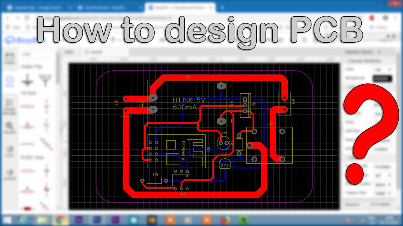
Then according to the circuit diagram, one by one I joined all the components. Now I have designed the PCB in a 2 layer format. That means we can make connections both on the top layer as well as the bottom layer. The top copper layer is denoted by Red path and bottom copper layer is denoted by the blue path.

Now, here the point to note is that, all the paths are turned at 45 deg. angle and secondly there are variable track width. Now what’s the reason behind these two points.
Why 45 deg.?
Not necessary for our small DIY projects but still every one practices this 45 deg angle in PCB. The reason which I was taught during my college days was. The electrons in motion emits radiation at sharp 90 degree curves and hence it may create interference in High frequency signals. Second reason they gave me was that during etching process there are more chances that the 90 degree curves get etched off easily while the 45 degree curves have less chances to get etched off during etching process. So these two reasons were taught me during my college days.
But if you ask me why I make this 45 degree curves is that the PCB looks great and professional with this 45 degree track curves.
Why variable track width?
We should use different track width for different current flow through that track. For High current, thick track and for low current thin pad. While searching online I got one table which you can use as a reference to decide your track width.

So with this image you can easily fig out the track width for your PCB.
After completely designing the PCB, we need to draw the outer border which will decide actual dimension of our PCB. The outer border is denoted by the purple path.

we can even curve the corners of our PCB easily. Now first of all save this file and and then click on the Generate fabrication file or we can say gerber file format on the top tools section.

Here comes the end of the tutorial on How to design the PCB on EasyEDA. Quite easy as it sounds. Now if you want to order PCBs online then we have an amazing website called JLCPCB.com
Just upload the Gerber file you just downloaded from EasyEDA and upload it on JLCPCB website.

Select the colour masking and pay for your order. You can get the amazing quality of PCBs at a very low price of $2 for 10 PCBs.
Still if you have any doubt regarding designing your own PCB, then watch out my full tutorial video on the same.