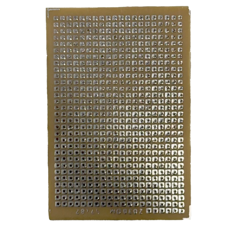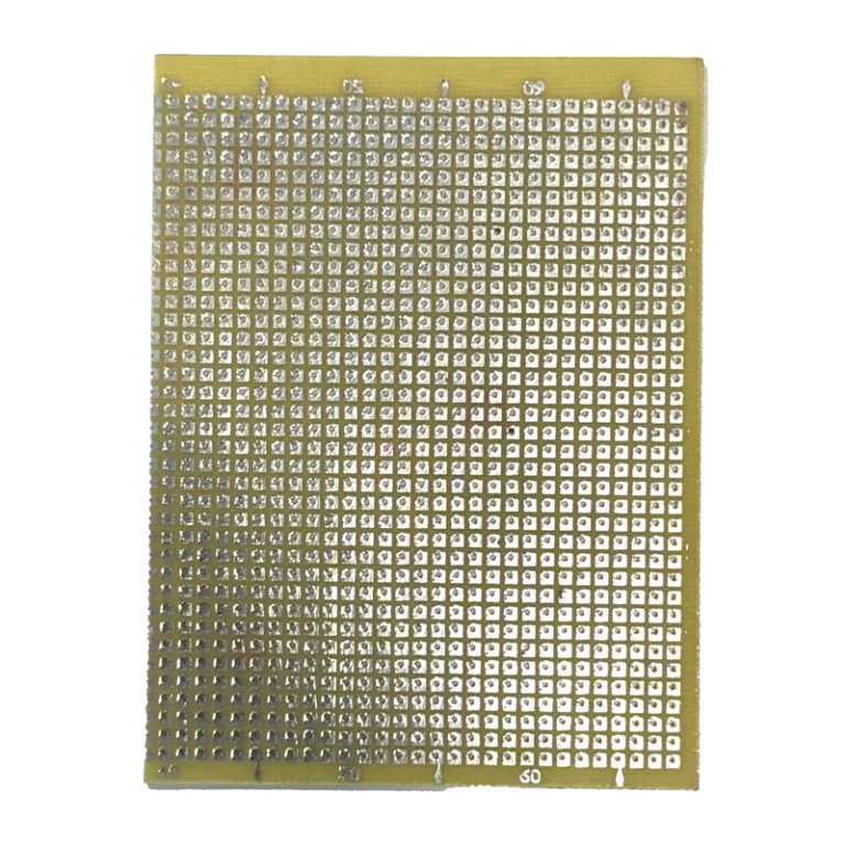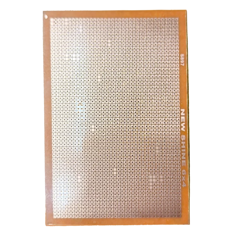
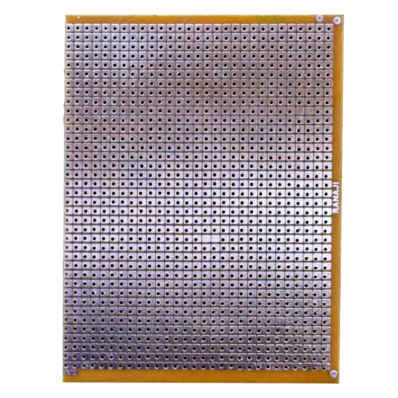
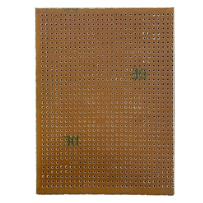

3×4 Inch Zero PCB Board (Copper Pads)

SKU: TDF2-005-1

A dependable copper zero PCB for Indian makers who want a permanent circuit build. Bare copper pads (not pre-tinned) give a stronger, cleaner solder joint than budget alternatives — ideal for prototyping, testing, and classroom soldering practice.

✅ Bare copper pads for stronger, direct solder bonds
✅ Standard 2.54mm hole pitch fits all through-hole parts
✅ Heat-resistant FR2 phenolic base survives repeated rework
✅ Compact 3 × 4 inch size, easy to handle and store
✅ Best price in India — only at techiesms

Apple Shopping Event

Hurry and get discounts on all Apple devices up to 20%

Sale_coupon_15

₹15.00
(inc. GST)

32 in stock

32 in stock

0 People watching this product now!

Payment Methods:

Description

Copper zero PCB boards like this 3 × 4 inch board give your circuit a permanent home once a breadboard layout is proven. Unlike pre-tinned boards, this one keeps its pads in bare, high-conductivity copper — the finish most Indian makers and students prefer for strong solder joints and reliable connections. It’s built for prototyping, testing, and custom circuit development where durability matters more than a shiny finish.

Technical Specifications

Here’s the full spec sheet for this copper zero PCB, verified against standard FR2 perfboard data used across the Indian electronics market.

ParameterValue
Board Size3 × 4 inches (75 × 100 mm approx.)
MaterialHigh-quality phenolic / FR2 board
Pad FinishBare copper pads (not pre-tinned)
Board Thickness1–1.6 mm
Hole TypePre-drilled, evenly spaced perforations
Hole Pitch2.54 mm (standard spacing)
Min. Hole Size0.3 mm
CompatibilityResistors, capacitors, ICs, sensors, connectors, and other through-hole components
Operating Temperature-10°C to 105°C (typical for FR2 phenolic substrate)

What Makes It Stand Out

Most beginner-grade boards ship pre-tinned, but that thin tin coating can make soldering trickier for anyone still learning heat control. This copper zero PCB skips that layer, so solder bonds directly to raw copper for a stronger, more consistent joint — useful when populating a board dense with ICs and headers.

The pre-drilled 2.54 mm grid means this copper zero PCB lines up perfectly with standard through-hole parts, including berg strip headers, without any measuring or redrilling. New to hand-soldering circuits? This zero PCB soldering guide walks through pad prep and joint technique.

The heat-resistant phenolic base also holds up to repeated rework, so you can revise a layout multiple times without pads lifting.

Why Makers Choose This

Students and hobbyists across India pick this copper zero PCB for a permanent build that still solders as easily as a breadboard prototype behaves. The uniform copper pads give a visibly cleaner joint than tin-finished alternatives, which matters when inspecting a board for cold joints or bridges during a workshop or exam project.

It also suits professionals who want a reliable surface between a breadboard test and a full custom PCB order — copper pads solder and desolder more predictably across revisions than tin.

Important Links

🔗 How to Solder Properly on Zero PCB — step-by-step video guide to pad prep and soldering technique
🔗 2×3 Inch Zero PCB Board — a compact-size option in the same board family
🔗 Male to Female Jumper Wires — for bridging this board to breadboards and dev boards during testing

Best Used For

This copper zero PCB is ideal for converting a working breadboard circuit into a permanent build — sensor projects, Arduino and ESP32 shields, power supply modules, and small robotics boards all benefit from its solid copper pads. It also suits college lab assignments and workshop kits where students practice clean, repeatable soldering, and makes a reliable base for point-to-point rework when repairing an existing device.

Frequently Asked Questions

Q: What’s the actual difference between copper pads and tin-plated pads?
Tin-plated boards have a thin tin layer over the copper for shelf appeal and short-term corrosion resistance. This copper zero PCB leaves the copper bare, giving a stronger direct solder bond that many experienced makers prefer.

Q: Is this board single-sided or double-sided?
This is a single-sided board — copper pads and traces are on one side only, standard for general-purpose prototyping boards at this size.

Q: Can I use SMD components on this board?
No — this board is designed for through-hole components with 2.54 mm lead spacing. Fine-pitch SMD parts need a different prototyping approach.

Q: Will the bare copper pads oxidize over time?
Some surface oxidation is normal with bare copper in humid Indian conditions, but it doesn’t affect solderability — a quick wipe or light flux restores a clean surface.

Q: Is this the best price for a copper zero PCB in India?
Techiesms prices this copper zero PCB at the best price in India, without compromising on board thickness or pad quality the way ultra-budget sellers often do.

Related Products

2×3 Inch Zero PCB Board
Male to Female Jumper Wires (20cm) – 40 Pieces
1×40 Pin Male Berg Strip – Break Away Header

Description

Copper zero PCB boards like this 3 × 4 inch board give your circuit a permanent home once a breadboard layout is proven. Unlike pre-tinned boards, this one keeps its pads in bare, high-conductivity copper — the finish most Indian makers and students prefer for strong solder joints and reliable connections. It’s built for prototyping, testing, and custom circuit development where durability matters more than a shiny finish.

Technical Specifications

Here’s the full spec sheet for this copper zero PCB, verified against standard FR2 perfboard data used across the Indian electronics market.

ParameterValue
Board Size3 × 4 inches (75 × 100 mm approx.)
MaterialHigh-quality phenolic / FR2 board
Pad FinishBare copper pads (not pre-tinned)
Board Thickness1–1.6 mm
Hole TypePre-drilled, evenly spaced perforations
Hole Pitch2.54 mm (standard spacing)
Min. Hole Size0.3 mm
CompatibilityResistors, capacitors, ICs, sensors, connectors, and other through-hole components
Operating Temperature-10°C to 105°C (typical for FR2 phenolic substrate)

What Makes It Stand Out

Most beginner-grade boards ship pre-tinned, but that thin tin coating can make soldering trickier for anyone still learning heat control. This copper zero PCB skips that layer, so solder bonds directly to raw copper for a stronger, more consistent joint — useful when populating a board dense with ICs and headers.

The pre-drilled 2.54 mm grid means this copper zero PCB lines up perfectly with standard through-hole parts, including berg strip headers, without any measuring or redrilling. New to hand-soldering circuits? This zero PCB soldering guide walks through pad prep and joint technique.

The heat-resistant phenolic base also holds up to repeated rework, so you can revise a layout multiple times without pads lifting.

Why Makers Choose This

Students and hobbyists across India pick this copper zero PCB for a permanent build that still solders as easily as a breadboard prototype behaves. The uniform copper pads give a visibly cleaner joint than tin-finished alternatives, which matters when inspecting a board for cold joints or bridges during a workshop or exam project.

It also suits professionals who want a reliable surface between a breadboard test and a full custom PCB order — copper pads solder and desolder more predictably across revisions than tin.

Important Links

🔗 How to Solder Properly on Zero PCB — step-by-step video guide to pad prep and soldering technique
🔗 2×3 Inch Zero PCB Board — a compact-size option in the same board family
🔗 Male to Female Jumper Wires — for bridging this board to breadboards and dev boards during testing

Best Used For

This copper zero PCB is ideal for converting a working breadboard circuit into a permanent build — sensor projects, Arduino and ESP32 shields, power supply modules, and small robotics boards all benefit from its solid copper pads. It also suits college lab assignments and workshop kits where students practice clean, repeatable soldering, and makes a reliable base for point-to-point rework when repairing an existing device.

Frequently Asked Questions

Q: What’s the actual difference between copper pads and tin-plated pads?
Tin-plated boards have a thin tin layer over the copper for shelf appeal and short-term corrosion resistance. This copper zero PCB leaves the copper bare, giving a stronger direct solder bond that many experienced makers prefer.

Q: Is this board single-sided or double-sided?
This is a single-sided board — copper pads and traces are on one side only, standard for general-purpose prototyping boards at this size.

Q: Can I use SMD components on this board?
No — this board is designed for through-hole components with 2.54 mm lead spacing. Fine-pitch SMD parts need a different prototyping approach.

Q: Will the bare copper pads oxidize over time?
Some surface oxidation is normal with bare copper in humid Indian conditions, but it doesn’t affect solderability — a quick wipe or light flux restores a clean surface.

Q: Is this the best price for a copper zero PCB in India?
Techiesms prices this copper zero PCB at the best price in India, without compromising on board thickness or pad quality the way ultra-budget sellers often do.

Related Products

2×3 Inch Zero PCB Board
Male to Female Jumper Wires (20cm) – 40 Pieces
1×40 Pin Male Berg Strip – Break Away Header

Specification

Overview

Processor

Display

RAM

Storage

Video Card

Connectivity

Features

Battery

General

Customer Reviews

0 reviews
0
0
0
0
0

There are no reviews yet.

Be the first to review “3×4 Inch Zero PCB Board (Copper Pads)”